
HBM Memory

The Dual Impact of HBM Reliability Test Standard Upgrades on Yield and Cost
High Bandwidth Memory (HBM) has moved into the mainstream of advanced computing, powering AI accelerators, high‑end GPUs, and cutting‑edge server platforms. As deployment scales and workloads become more demanding, the industry has steadily tightened reliability expectations for HBM devices. This has led to upgraded reliability test standards across thermal, electrical, mechanical, and system‑level dimensions.

HBM4 Mass Production Kickoff: The 2026 Tech Roadmap Showdown Among 3 Memory Giants
By 2026, high bandwidth memory (HBM) has moved from a niche enabler of premium accelerators to a central battleground in the AI and advanced computing industry. The kickoff of HBM4 mass production marks a decisive escalation: the three leading memory giants are no longer just supplying components; they are effectively shaping the performance envelope and cost structure of the next generation of AI chips.

Interpreting the Capital Market Signals of Samsung’s HBM3E Nvidia Certification
Samsung’s public announcement that its HBM3E modules achieved Nvidia certification is more than a product milestone—it sends multi-layered signals to capital markets about demand, competitive positioning, supply-chain dynamics, and future cash flows across memory makers, OSATs, accelerator OEMs, and equipment vendors.
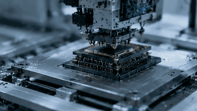
TSV Technology Iteration in HBM – New Requirements for Equipment Suppliers
Through successive HBM generations the through-silicon via (TSV) has evolved from a tactical enabling feature into a strategic differentiator. As HBM moves from HBM2E and HBM3 to HBM3e and HBM4, TSVs must support finer pitches, lower parasitics, higher thermal conduction needs, and coexistence with hybrid-bond planes. These requirements cascade into new expectations for equipment suppliers across lithography, etch, deposition, CMP, inspection, and metrology.
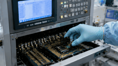
Incremental Demand for HBM Test and Burn-in Equipment – A Quantified Forecast
As High-Bandwidth Memory (HBM) moves from niche to mainstream across AI, HPC, and advanced graphics, test and burn-in equipment emerges as a critical bottleneck. HBM modules require more extensive, higher-fidelity testing than commodity DRAM: multi-die functional tests, high-speed channel validation, thermal stress profiles, and system-level burn-in under representative accelerator loads.

Hybrid Bonding Adoption in HBM4 and Its Supply Chain Opportunities
Hybrid bonding—a suite of direct copper-to-copper and copper-to-dielectric bonding techniques—has become central to the HBM4 roadmap. Where previous HBM generations relied primarily on micro-bumps and through-silicon vias (TSVs), HBM4 pushes signaling density and electrical performance to levels that make hybrid bonding not optional but essential.

Global HBM Patent Landscape Competition: The US-China-Japan-Korea Power Game
High-Bandwidth Memory (HBM) has become one of the most strategically important technologies in the AI and high‑performance computing era. Patents around HBM architectures, hybrid bonding, TSVs, interposers, thermal solutions and test methods now form a dense web of intellectual property that shapes who can manufacture, license and profit from AI memory at scale. The global HBM patent landscape is increasingly a power game among the United States, China and Japan, layered on top of Korean and Taiwanese industrial strengths.

HBM’s Value Share Per AI Server Unit Continues to Rise
High-Bandwidth Memory (HBM) has steadily transitioned from a niche premium to a core system-level enabler for modern AI servers. As models grow larger and throughput demands intensify, designers increasingly attach value to bandwidth, density, and energy efficiency that HBM uniquely provides.

Breakthroughs in Wafer Warpage Control During HBM Manufacturing
Wafer warpage has long been a critical yield and reliability concern in advanced semiconductor packaging, and it is especially consequential for High Bandwidth Memory (HBM). HBM’s stacked-die architecture, use of through-silicon vias (TSVs), and reliance on precise bonding and micro-bump formation all amplify the impact of any deviation from flatness. Recent breakthroughs in warpage control—spanning materials science, process engineering, metrology, and modeling—are improving yields, reducing costs, and enabling larger HBM stacks with higher interconnect densities.
Big 3 Memory Makers’ HBM CapEx Share Exceeds 50% for the First Time in 2026
In 2026 the semiconductor landscape reached a decisive inflection: the combined capital expenditure (capex) directed by the industry’s Big Three memory makers—SK Hynix, Samsung, and Micron—toward High-Bandwidth Memory (HBM) and its enabling packaging technologies exceeded 50% of total industry HBM-capex for the first time. This milestone matters because it signals concentrated investment toward premium memory and packaging ecosystems that underpin AI accelerators, HPC clusters, and advanced datacenter architectures.

Post-HBM4 Roadmap: A Forward Look at HBM4E and HBM5 Specs
As HBM4 moves from pilot to early volume, industry attention is already shifting toward the next logical stages: evolutionary refinements sometimes labeled HBM4E and a more disruptive generational step often discussed under the HBM5 moniker. This post surveys likely technical directions, realistic performance and integration targets, key enabling technologies, supply-chain and manufacturing implications, and design trade-offs system architects should expect over the next 3–6 years.

The Structurally Upward Shift in Memory ASP Driven by HBM
High Bandwidth Memory (HBM) has become a defining technology in modern computing architectures. As HBM adoption grows across GPUs, AI accelerators, and high-performance CPUs, it is doing more than just increasing raw throughput. HBM is driving a structural upward shift in the memory Application Service Profile (ASP)—the way systems expose, package, and price memory as part of broader computing platforms.

Analyzing the Possibility of New Entrants Challenging the HBM Oligopoly
High Bandwidth Memory (HBM) has become central to high-performance computing, AI accelerators, and advanced graphics. Its market is currently dominated by a small number of players with deep expertise in DRAM design, advanced packaging, and system-level integration. This concentration has led many to describe HBM as an oligopoly.

A Full Mapping of HBM-Themed Targets in the A-Share Market
As High-Bandwidth Memory (HBM) becomes a core enabler for AI, high-performance computing and advanced graphics, China’s domestic capital markets have seen a rapid expansion of “HBM concept” stocks and supply-chain plays. While the most advanced HBM die and module production remains concentrated in Korea and the United States, a growing number of A-share listed companies participate in the broader HBM ecosystem—through equipment, materials, packaging, substrates, thermal solutions, and peripheral components.

The Layer Stack and Thermal Bottleneck Breakthroughs in the HBM3E-to-HBM4 Upgrade
Upgrading from HBM3E to HBM4 represents one of the most technically challenging—and most consequential—evolutions in modern memory engineering. HBM4 promises higher signaling rates, greater per-die capacity, and improved energy efficiency per bit, but achieving those gains requires rethinking the layer stack, interconnect strategies, and thermal management at the package level.

Tracking the Spot vs. Contract Price Spread Dynamics in HBM Market
High-Bandwidth Memory (HBM) has transitioned from a boutique, high-margin specialty to a strategic commodity within high-performance computing and AI infrastructure. That transition created two distinct pricing channels: spot-market transactions (ad-hoc purchases, inventory sales, and opportunistic trades) and contract-based procurement (multi-year supply agreements, prepayments, and capacity reservations).

2027 HBM Market Size Forecasts: The Upper/Lower Bound Divergence Among Major Institutions
High Bandwidth Memory (HBM) has transitioned from a niche technology to a central pillar of the AI and high‑performance computing ecosystem, and by 2027 it is expected to sit at the heart of GPU, accelerator, and advanced CPU platforms worldwide. Against that backdrop, financial institutions and industry research houses have been racing to forecast the market size for HBM, yet their estimates vary widely. Some project an aggressive, multi‑fold expansion with tight supply and premium pricing, while others caution that bottlenecks and substitution effects could cap growth.

2026 HBM Supply-Demand Gap Forecast: How Much Shortfall Remains?
High‑Bandwidth Memory (HBM) is now a critical component across AI training clusters, inference accelerators, and high‑performance computing systems. As demand surged between 2022 and 2026, suppliers scrambled to expand wafer capacity, interposer production, advanced packaging, and specialized test and burn‑in capacity. Yet multiple bottlenecks—packaging throughput, materials, tooling lead times, and yield learning—left the market short of fully meeting demand.
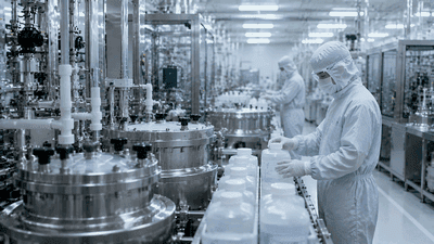
The Irreplaceability of Japanese Material Suppliers in the HBM Supply Chain
High-Bandwidth Memory (HBM) has quickly become a strategic pillar of modern AI, HPC, and accelerator architectures. Behind the headlines about wafers, interposers, and packaging capacity lies a quieter but crucial reality: a small cluster of highly specialized Japanese material suppliers provides many of the chemicals, precision films, specialty substrates, and consumables that enable reliable, high-yield HBM production.
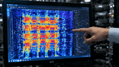
HBM Power Consumption and Thermal Issues Become Core System-Level Design Bottlenecks
High-Bandwidth Memory (HBM) has become essential for modern AI accelerators and high-performance compute nodes because it delivers massive on-package bandwidth and high energy efficiency per bit transferred. Yet as HBM stack counts, per-die speeds, and module counts per accelerator increase, power consumption and thermal management move rapidly from component-level concerns into system-level bottlenecks.
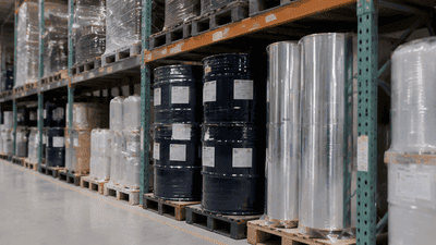
Critical Auxiliary Material Shortages in HBM Supply Chain: GMC and EMC Supply Gaps
High-Bandwidth Memory (HBM) adoption accelerated rapidly between 2022 and 2026 as AI, HPC, and advanced graphics drove demand for on-package, ultra-high-bandwidth memory. While attention has rightly focused on wafer and packaging capacity—fabs, interposers, and OSAT lines—another set of constraints has quietly become a systemic risk: shortages in key auxiliary materials, notably gas-phase metal-containing chemicals (GMCs) used in advanced deposition and surface treatments, and electrically conductive/thermally managed materials (EMCs) used in thermal interface and conductive adhesives.

Calculating HBM Capacity Demand for Nvidia B200: How Many GB Per Chip?
As AI models scale into the multi‑trillion‑parameter era and context windows stretch into hundreds of thousands of tokens, memory capacity has quietly become as important as raw compute for accelerators like Nvidia’s B200. When architects and investors ask, “How many GB of HBM does a B200 really need per chip?” they are not just hunting for a spec sheet number; they are trying to understand how memory sizing interacts with model sizes, cluster design, and total cost of ownership.

China’s HBM Localization Progress: The Catch-Up Pace of CXMT and XMC
China’s drive to localize advanced memory technologies has accelerated over the past several years. High-Bandwidth Memory (HBM) sits near the center of that strategy because it is integral to AI accelerators, high-performance computing (HPC) and other strategic compute platforms. Two domestic players—ChangXin Memory Technologies (CXMT) and XMC (Xianghui Memory, commonly referred to as XMC)—have become focal points in assessing how quickly China can close the gap with international incumbents on HBM die, stacking, and packaging.

The HBM Capacity Expansion Race: SK Hynix, Samsung, Micron 2026 Capacity Map
In 2026 the high-bandwidth memory (HBM) market sits at a strategic crossroads. Driven by generative AI, large language models, high-performance computing (HPC), and advanced graphics, demand for stacked memory with ultra-high throughput continues to surge. This post maps the 2026 HBM capacity expansions from the three dominant players—SK Hynix, Samsung, and Micron—examines their strategies, regional footprints, technology choices, and the implications for customers, OEMs, and the supply chain.

HBM’s Crowding-Out Effect on DRAM Capacity: Supply Tightening Supports Traditional DRAM Prices
Between 2023 and 2026 the semiconductor industry witnessed a structural shift: a growing fraction of global DRAM wafer-equivalent capacity was repurposed for High-Bandwidth Memory (HBM) production. That reallocation—driven by hyperscaler commitments, higher ASP incentives, and strategic capex by major memory makers—has had a pronounced “crowding out” effect on commodity DRAM supply.

HBM’s Gross Margin Far Exceeds Traditional DRAM – A P&L Repair Effect for Memory Makers
High-Bandwidth Memory (HBM) has evolved from a niche, premium product to a strategic revenue generator for memory manufacturers. Compared with commodity DRAM, HBM commands higher average selling prices (ASPs), deeper integration services, and packaging premiums that lead to significantly superior gross margins. For memory makers facing cyclical commodity DRAM pricing and margin compression, HBM presents a meaningful “P&L repair” lever—a way to improve profitability, stabilize revenue mix, and insulate firms from the worst swings in the DRAM cycle.

HBM Re-rated from Cyclical to AI Growth Asset – A Valuation System Overhaul
High Bandwidth Memory (HBM) has long been categorized alongside other DRAM products as part of a cyclical commodity business, subject to booms and busts driven by general compute and consumer demand. In the AI era, that classification is increasingly inaccurate. As accelerators for training and inference depend more deeply on HBM for performance and energy efficiency, the asset’s economic profile is shifting from cycle-sensitive to structurally supported by long-term AI growth. This re-rating of HBM—from cyclic memory component to AI growth asset—forces a rethink of how investors, companies, and policymakers value and manage it.

Customer Concentration Risk in HBM: Over-Reliance on a Single AI Giant
High-Bandwidth Memory (HBM) sits at the heart of modern AI infrastructure. A small group of hyperscale cloud and AI platform providers now buys a very large share of global HBM output, often through multi‑year contracts and co‑investment arrangements. This buying power has helped finance HBM capacity expansion—but it has also created a new kind of risk for memory makers, OSATs, material suppliers and equipment vendors: extreme customer concentration.

The Bundled Investment Thesis of HBM and CoWoS: Indispensable Pair
In modern high-performance computing and AI system design, High-Bandwidth Memory (HBM) and Chip-on-Wafer-on-Substrate (CoWoS) packaging have evolved from complementary technologies into a tightly coupled investment thesis. This post examines why investors, system architects, and policymakers should view HBM and CoWoS as an intertwined opportunity—how technological synergies, supply-chain economics, customer demand patterns, and geopolitical dynamics create a single strategic story rather than two separate bets.
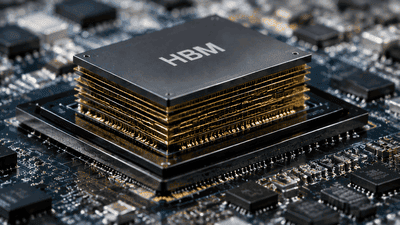
HBM’s Share of Global DRAM Capacity Exceeds 20% for the First Time in 2026
In 2026 the semiconductor industry recorded a milestone: high-bandwidth memory (HBM) has crossed the 20% threshold of global DRAM wafer-equivalent capacity for the first time. This is not merely a metric—it's a structural signal. It reflects changing customer priorities, deliberate capital allocation decisions by leading memory makers, and maturation of advanced packaging ecosystems that finally translate wafer output into finished, high-value modules at scale.